Naresh Koirala
SpO2 Monitoring Project
PCB Design & Software Integration

Summary
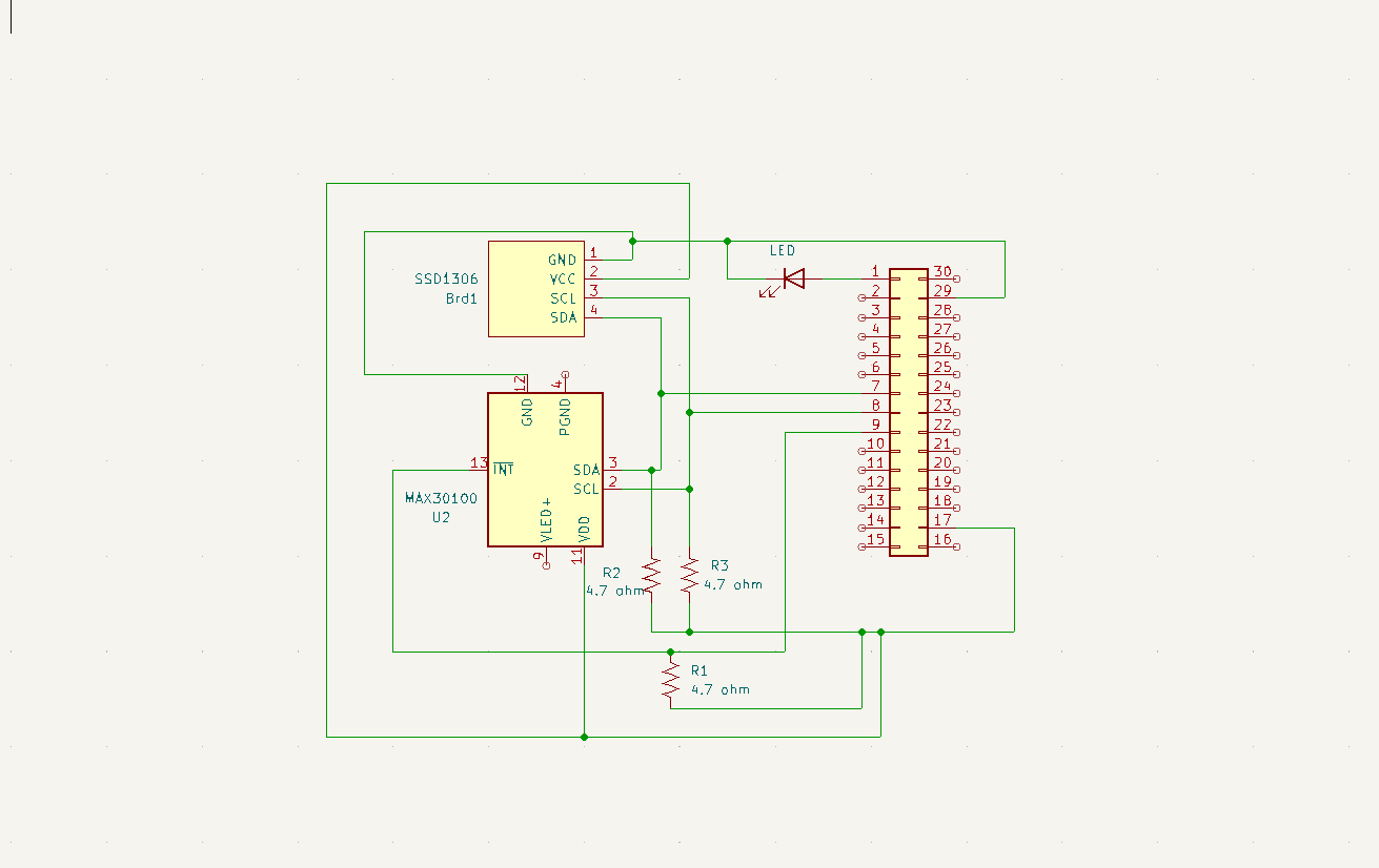
Initiated the project with a breadboard prototype to verify the functionality of critical components, utilizing I2C communication via SDL and SDA pins to connect an OLED display and a MAX30100 sensor in a bus configuration. A 255-bit loop test was implemented, leveraging pre-existing GitHub libraries for the OLED and sensor, to validate component communication with the microcontroller (MCU). The test confirmed successful I2C address recognition, verifying the operational integrity of the components.
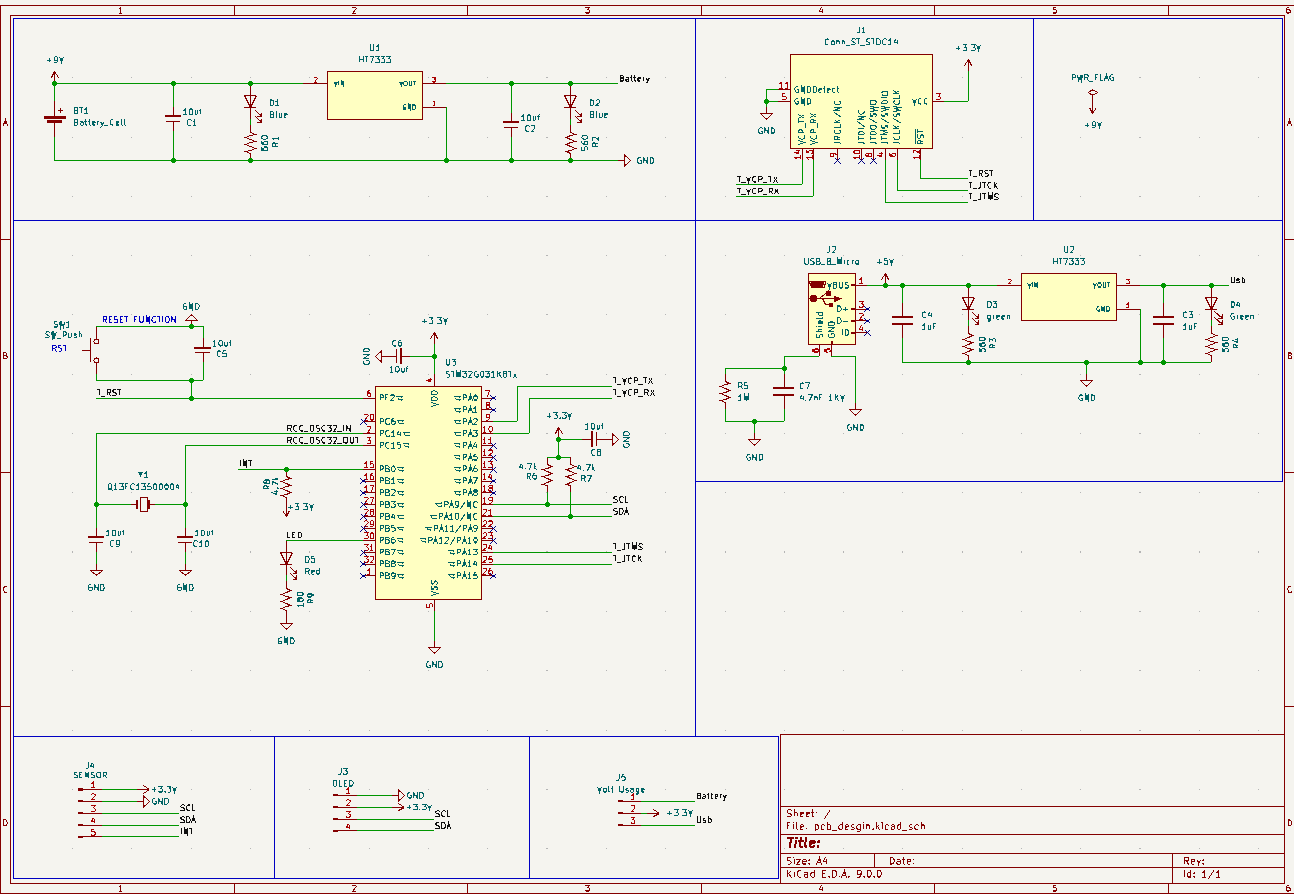
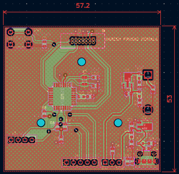
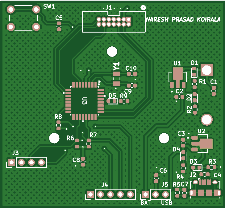
Subsequently, a schematic was developed in KiCad, optimizing the breadboard design by streamlining the required pin connections. This led to the iterative design of a dual-power-rail PCB, incorporating a 9V battery rail and a USB-powered rail with an ST-LINK interface for debugging. The PCB includes a robust power monitoring system, featuring four LEDs—two per rail—to provide visual confirmation of power status at multiple checkpoints, ensuring reliable operation across both power sources. After completing the schematic, multiple PCB design iterations were evaluated, culminating in a finalized design. The final PCB layout was then submitted to JLCPCB for fabrication.
Tools Used
- STM-Cube IDE (Programming)
- HAL
- C
- KiCad 9.0
- PHP
- KiCad
- SSD1309 (OLED)
- MAX30100 Sensor
- STM32G0
Breadboard Design
The initial breadboard prototype was designed to test the core functionality of the SpO2 monitoring system, focusing on I2C communication between the MCU, OLED display, and MAX30100 sensor.

KiCad (Schematic + PCB) Design
The KiCad schematic optimized the breadboard layout, reducing pin connections and enabling a dual-power-rail PCB design with robust power monitoring and debugging capabilities.
Software Implementation
The software was developed using STM-Cube IDE, leveraging HAL and C to manage I2C communication and sensor data processing, with additional open source libraries used for additional functionality.
Soldering/Desoldering
The final PCB assembly involved precise soldering of components, with desoldering techniques applied during iterations to refine the design and ensure reliability.